
The quest for greater conductivity in semiconductors for microelectronics devices has led University of California engineers to the creation of the world’s first semiconductor-free microelectronic device. The device, which uses “metamaterials” in its construction, tested with a 1,000 per cent increase in conductivity when activated by low voltage and a low-power laser. The UC engineers say the breakthrough paves the way for faster, more powerful microelectronic devices and possibly even more efficient solar panels.
In explaining their work, the engineers note that the conductivity of microelectronic devices is limited by their constituent materials, including semiconductors. Semiconductors put up resistance to the flow of electrons as well as requiring jolts of energy to trigger their conductivity. These semiconductor “pitfalls” can be problematic for microelectronic components like transistors. Whereas large electronic devices made with large semiconductor components can withstand the jolts of energy, strong laser pulses and high temperatures necessary to start conductivity, smaller components cannot.
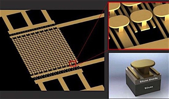
Their solution “sidesteps” the limitations of conventional semiconductor materials by using instead metamaterials, consisting of gold, table-like nanostructures that are etched onto an array of gold strips. These are attached to a silicon wafer, buffered by a layer of silicon dioxide.
With less than 10 volts of power and a low-power laser applied to the metasurface, the gold nanostructures generate intense electric fields, called “hot spots,” that are strong enough to decouple, or liberate, electrons from the material. These electrons can then move about uninhibited, without resistance.
Extracting electrons from a material so that they can move freely in either a gas plasma or vacuum is “challenging,” the engineers note, often requiring heating to high temperatures or the use of high-power lasers. Their process shows that low-power infrared laser can cause sufficient photoemission to implement “feasible” microelectronic devices such as transistors and switches.
The engineers say that their device may be the best approach for certain “specialty” applications, such as high-power devices. The next step is to understand how the devices can be scaled, and the limits of their performance.


